
The SM-2010 Project: The System Clock
Time has Come today (Time!)
I might get burned up by the sun. But I had my fun. My apologies to the Chambers Brothers for that heading, but that line has particular meaning to anyone who has pored over timing chart after timing chart before embarking on a Quixotic tilt at a CMOS windmill. I envision millions out there that have done just that.
The SM-2010 is nothing if not clocked up one wall and down the other. But, with all the counters required for it to actually do what it is intended to do, that's not surprising.
Seriously, though, a number of things had to be considered, hashed out, trashed, considered and hashed out again while figuring out how to clock the behemoth.
For starters, the clock would have to be very fast (I'm not talking about modern-computer-clock-rate fast, but fast in comparison to things I've had to clock in my own projects). The architecture I've settled on requires that the entire pattern is to be read from RAM with each step of the sequence, and each edit requires that the entire pattern be written to RAM before that read function. My goal is that a single read operation occurs within 1 ms and a single write operation occurs within 1 ms. In other words, the 128 bits of data that are contained within a pattern must be written or read in 1 ms (0.001 S). This concept of the timing was as good of a starting point as any for determining the clock frequency: simply put, one need only divide 1 ms by 128, then divide that into 1 to get to the system clock frequency:
1/(0.001/128 = 0.0000078125) = 128000, or 128 kHz. Great! Now I have my system clock frequency.
But, as I proceded down the slippery slope of the project, I realized that a simple system clock just wasn't going to easily handle the complex timing required for clocking the counters, shift registers and timing signals required to interface the data to RAM (and pull off various and other sundry duties). I would need separate sets of very fast sequences of pulses, offset in time yet synchronized, to sequentially pull off these tasks. So, I settled on creating the three phase clock system: Three streams of pulses offset in time to each other. It goes something like this.....
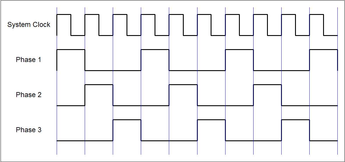 |
This is exactly what the doctor ordered. Each phase of the clock is sequential - one phase can complete a function, then wait while the other two phases complete their functions before repeating the function dedicated to the referenced phase. It may or may not, technically, be a three phase clock, but "three phase clock" is a lot easier to write repeatedly than "that circuit with the three sequential outputs".
Well....anyway....looking at Figure 1, it becomes very obvious that each phase occurs once for every three ticks of the system clock. In other words, the system has now slowed down to one third the frequency of the system clock. These signals are to be used for implementing the RAM I/O operations, clocking the counters and so on and so forth, so the system clock must now be tripled in order to accomodate this scheme. The original system clock calculation of 128 kHz must now be bumped up to 128 kHz * 3, or 384 kHz. Therefore, each phase of the system clock will operate at 128 kHz.
Implementing the Three Phase Clock
If one thinks about it for any length of time, the phase outputs of the system clock resemble the output of a simple three step sequencer. One of the most ubiquitous simple DIY sequencers is, of course, the Baby 10 sequencer, which is based around the CD4017 Divide-By-Ten counter, and that is exactly what I use (though, in truth a CD4022 would work just as well, I just happen to have an abundance of CD4017s lying around here).
 |
The implementation is quite straight-forward: the master system clock is applied to the clock input of the CD4017. Q0 forms the phase 1 output, Q1 forms the phase 2 output, and Q2 forms the phase 3 output. Q3 is connected to the reset input, so as soon as the 4017 advances the count from Q2 to Q3, it immediately resets back to Q0. Thus, the 4017 outputs only three sequential pulse trains continually. It's really quite simple, and it's a pity that three phases just isn't enough......
Subdivisions
Actually, what I found as I was working out the scheme of this whole project was that I really, really needed more sequential pulses than just the three provided by the three phase clock. However, I really was not all that keen on upping the clock frequency any more, because I did actually need clock signals of the width the three phase pulses provided. Fortunately, there is an additional maneuver that allows each of the three phases to be divided down into two additional phases, making this, essentially, a six phase operation.
In order to split each output of the three phase clock into two separate pulses, the system clock is ANDed with the phase output to form the first subdivision and the inverted copy of the system clock is ANDed with the phase output to form the second subdivision.
 |
If you look at Figure 1, you'll notice that for as long as each phase output stays high, the system clock stays high for the first half of the phase duration, and drops low for the second half of the phase duration. Therefore, in Figure 3, one can see that ANDing the system clock with Phase 1 produces a waveform that is high during the first half of the Phase 1 signal. This output is called "Phase 1 Pulse 1".
When the system clock is inverted, the inverted system clock is high during the second half of the Phase 1 pulse. Thus, ANDing the inverted system clock signal with the Phase 1 signal produces a waveform that is high during the second half of the Phase 1 signal. This output is called "Phase 1 Pulse 2".
Performing this operation on each phase of the three phase clock theoretically produces six separate, sequential outputs, as can be observed in Figure 4.
 |
So, now there are six separate sequential pulses that can be used to generate all the particular timing signals for all of the low-level functions of the SM-2010 sequencer. Because each subdivision is coincident with the phase from which it is derived, there is no need to alter the clock frequency any further. This would be perfect, except that it doesn't quite work as drawn.
Kicking the Propagation Delay Blues
In a world where rise and fall times are truly instaneous, just relying on the AND gates to create the subdivisions would likely work fine and dandy, but that doesn't happen to be the world we live in. Instead, everything has a finite rise and fall time, and, as fast as CMOS is, it still will move slow enough for an AND gate to tag that fleeting high glitch right when you would quite rather it didn't.
In Figure 2, we see that the system clock is driving the CD4017, which is creating the individual phase outputs. The 4017 clocks forward on every rising pulse, but it doesn't do it instantly - there is a period of time between when the the system clock rises and when the 4017 shifts its output from one Q to the next Q. This period of time is the propagation delay, and can be measured in hundreds of nanoseconds when operating at 5 Volts, which this circuit is (higher voltage supplies result in lower propagation delays, but we need 5V operation to play nice with the RAM). During the propagation delay, the system clock signal is high before the Q signal it's supposed to bring low actually goes low as the Q transfers to the next Q output. In other words, during that period of propagation delay, both the system clock and the Q output are high when we don't want them both to be high. Stupid physics....
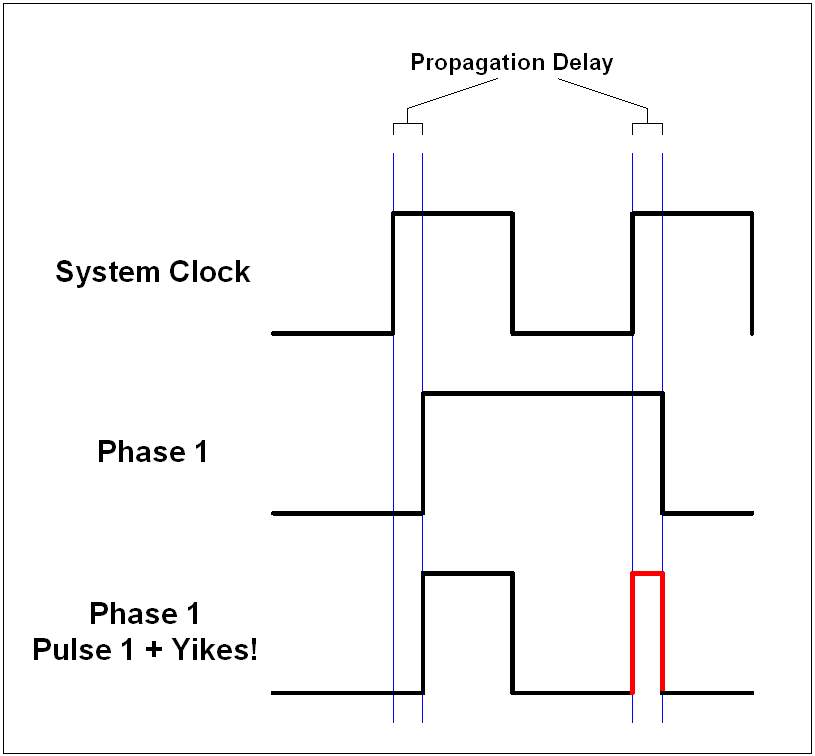 |
In Figure 5 we can see just how this propagation delay can really spoil one's day. The System Clock signal rises, which brings the Phase 1 pulse high. Notice there is a time delay between these two events (the first propagation delay). The propagation delay is shown a bit larger than real life in Figure 5 just to make things a bit more clear. One can see that the propagation delay shaves a bit of time off of the Phase 1 Pulse 1 signal, because it does not go high until after the propagation delay. A slightly thinner pulse is not much of a problem to deal with. It's what happens on the other side of the diagram that's the killer.
When the System Clock signal goes high again to move the Q output down the line of the CD4017, the signal doesn't actually move until after the propagation delay. In that period, both the System Clock signal and the Phase 1 signal are high. Remember - these two signals are being fed to a CD4081 AND gate, which doesn't have nearly the delay that the 4017 does (the 4017 has a bit more plumbing for the internal signals to run through). So, because, during that brief instant, both signals are high, the AND gate says "I spy!" and dutifully sends its output high because, after all, both of its inputs are now high. Right the hell after that, of course the Phase 1 signal does drop low as the 4017 lumbers along, and the AND gate drops low; one of its inputs is now low, so it is only doing its duty. But, of course, this is after the swollen, red Yikes! pulse has been generated by the vigilant AND gate.
This extra pulse is death to any circuit that relies on clocked logic, the type of logic this project relies on in ambundance. Obviously, all the phase pulse 1's will have their own Yikes! pulse. The Yikes! pulse must go, otherwise the SM-2010 device will do nothing but jibber random, haphazard pulses from its outputs for its short, miserable life.
So...what to do? Well, what I decided to do was to pass each of the 4017 outputs through a Schmitt trigger one-shot circuit before being ANDed with the clock signals. The RC time constants of the Schmitt triggers artificially shorten the time the 4017 outputs remain high.
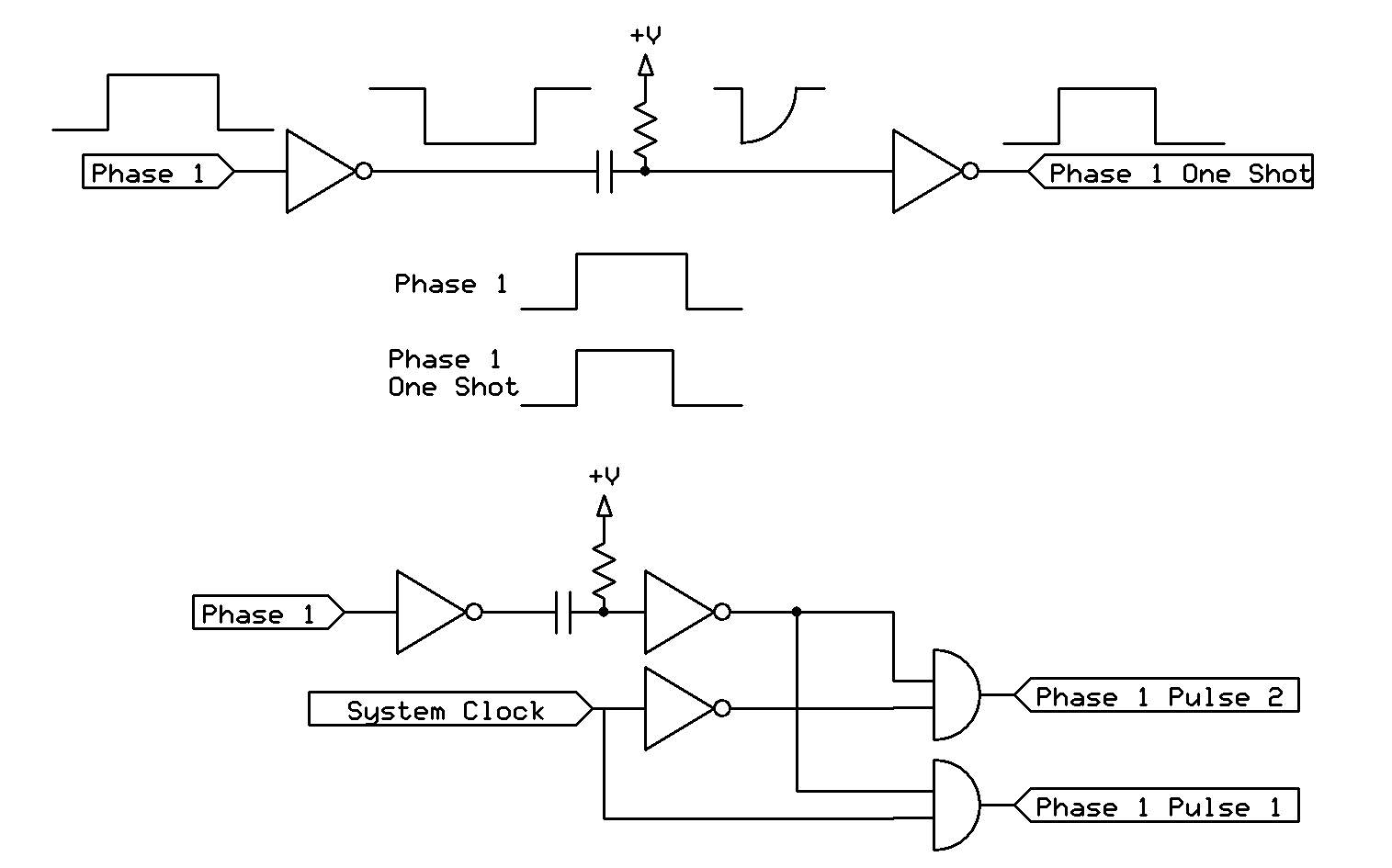 |
Anyone who has looked at my tortured designs will recognize my love of the Schmitt trigger one-shot. It's such an invaluable tool to have around. I use either a CD40106 or CD4534 Schmitt trigger for my one-shots (the two devices are, for all practical purposes, identical).
To review what the one shot is doing, note that, with no pulse present on the input of the first inverter, the output of that inverter is high. The second inverter has a positive voltage tied to it through the resistor, so the output of the second inverter is low (when no signal is present). When the first inverter input goes high, its output snaps low. This high to low transition sucks the juice out of the capacitor, which pulls the second inverter's input low and snaps its output high. Ah...but the capacitor is being fed voltage, and the resistor allows current to trickle through, charging the capacitor back up. Once the voltage on the cap builds up to the Schmitt trigger point, the output of the second inverter snaps low again, regardless of the fact that the voltage on the input of the first inverter is still high. The RC values of the resistor/capacitor determine how long this pulse will last (as long as the input pulse is wider than the desired output pulse). Thus, we create a shorter pulse out of a longer pulse. And that's certainly what we want here.
Because the Phase 1 signal is now shortened by the one-shot before being ANDed with the system clock, it goes low before the system clock tells it to go low. It goes low before the propagation delay can wreak its deadly havoc. No deadly havoc, no more swollen, red Yikes! pulse to deal with.
Of course, this procedure is performed on all three of the CD4017 Q outputs.
The Complete System Clock Circuit
Figure 7 details the Three Phase Clock as I have it currently implemented. In the schematic, it is labeled as the TriPhase Counter, in keeping with my campaign to make things as complicated as possible.
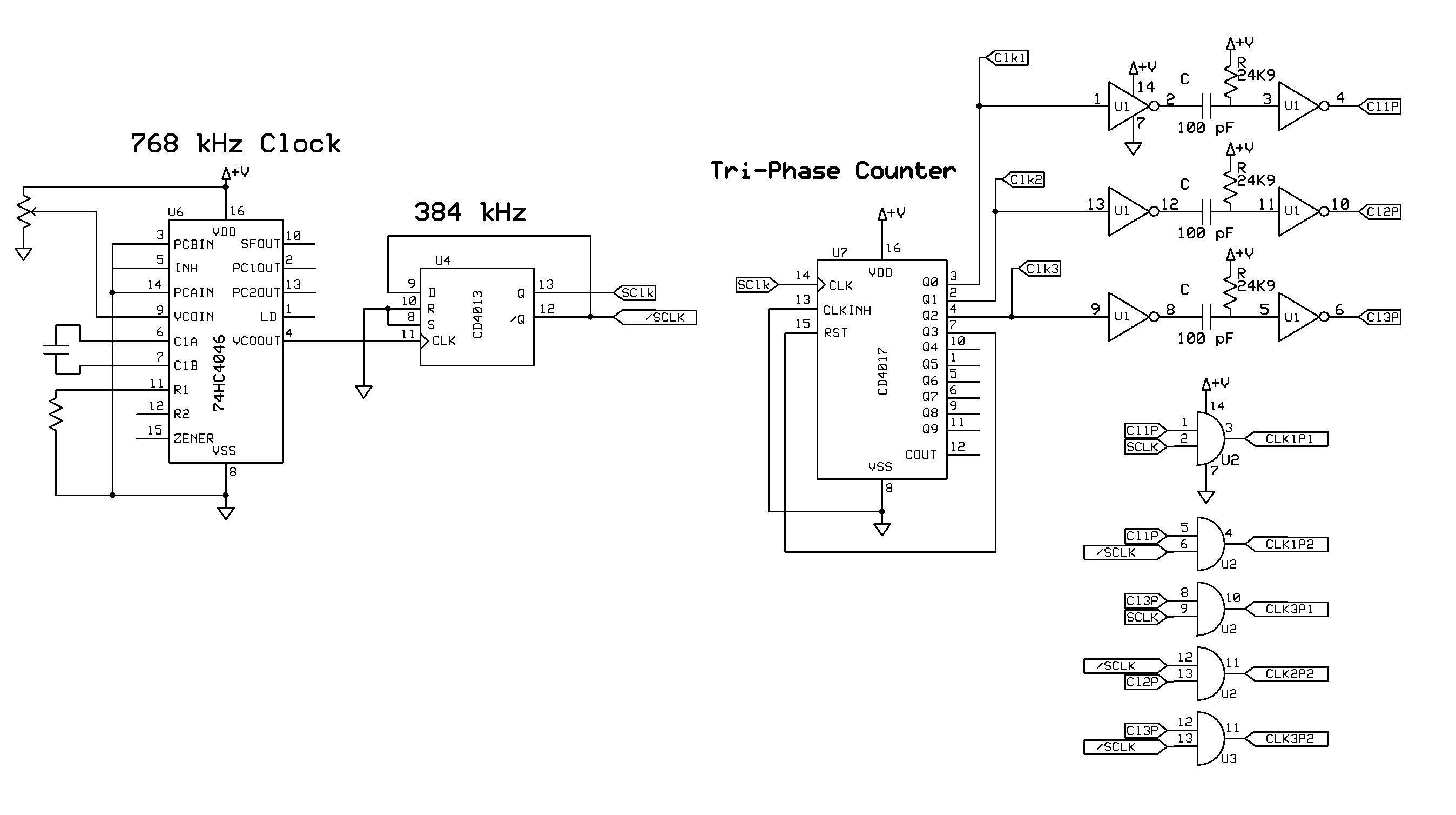 |
You'll likely note that the 74HC4046 (U6) is set to produce 768 kHz rather than 384 kHz. The reason for this is, I wanted to be absolutely sure that the system clock duty cycle is as close to 50/50 as possible - this is absolutely crucial. Flip-flop U4 performs this task, and, in the process, divides the frequency by two down to the target 384 kHz. I did consider using the on-board XOR gate of the 74HC4046 to provide the inverted copy of a 384 kHz clock signal, instead of operating at the higher frequency, but I really just did not want to leave the duty cycle in the hands of the 74HC4046, so to speak.
The system clock tag is "SCLK". The /Q output of the flip-flop provides the inverted system clock signal, "/SCLK".
The original phase outputs of the CD4017 are used in the circuit. They are labeled as CLK1, CLK2 and CLK3, respectively.
The one shot versions of the CLKn pulses are labeled CL1P, CL2P, and CL3P.
The subdivisions are labeled CLK1P1, CLK1P2, CLK2P2, CLK3P1, and CLK3P2. Note that there are actually only five subdivisions, not six - there is no use in the following circuitry for a CLK2P1 signal, so it is not generated.
Signal Specifics
Knowledge of the timing parameters of the 3 Phase System Clock section is critical to understanding a good deal of the entire project. Following are the pertinent specifications:
System Clock (SCLK) Frequency: 384 kHz
System Clock (SCLK) Cycle Width: 2.6 us
System Clock (SCLK) High Width: 1.3 us
System Clock (SCLK) Low Width: 1.3 us
/SCLK Properties are Identical to SCLK
CLK1, CLK2, CLK3 Signal Properties:
Frequency: 128 kHz
High Width: 2.6 us
Low Width: 5.2 us
Subdivision (CLk1P1, CLK1P2, CL2P2, CLK3P1, CLK3P2) Frequency = 128 kHz
Subdivision (CLk1P1, CLK1P2, CL2P2, CLK3P1, CLK3P2) High Width = 1 us
And that, dear reader, is the system clock portion of the SM-2010 Matrix Sequencer