
Prototyping The SM-2010
Getting a Handle on the Beast
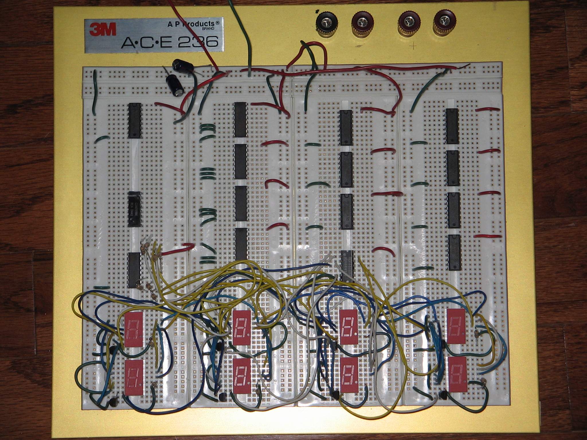
The SM-2010 is, by far, my most ambitious (crazy?) project yet. At this writing, I've only posted a trifling of schemata detailing exactly how much circuitry is involved. It's a lot.
There are several functional blocks of the device. A small portion of it is fairly easy to breadboard and test on an individual basis. For example, it's a comparatively trivial matter to breadboard the system clock and get it up and running, and portions of the control counter can be tested without having some other section driving them. But, generally, those individual, testable sections are really very few in number. A lot of the functions require some other function to be up and running, and that other function needs another function in order for it to operate and....that function will need the target function to be running in order to for it to run. Chicken, meet egg.
The plan of attack is to get together smaller portions of larger circuits together, and go/no-go test them. Other tests may require the setup of test circuits to ensure they'll be cricket when I actually interface the section under test to the actual circuitry.

This phase of the design is fairly difficult, put probably not nearly as difficult as dividing up the functions into various boards and interfacing them together, but that's another subject. This page is about the actual breadboard prototyping of the device.
I'll update this page as things progress. If anything new is added, it'll show up as a link in the little gray box in the upper left of this page.
This is going to take a while. I'm without help, as you can plainly see that Igor, my lab assistant, has recently been afflicted with some sort of flesh-eating malady that renders his contributions more or less ineffective
That's a switch
One thing this device uses plenty of is momentary SPDT push-button switches. Normally, when I breadboard any control, be it a pot or a switch, I'll solder wires to it and let it wobble around above the fray of the breadboard. But, in this case, there are better than twenty push-button switches, and it's going to take more RAM in my brain than is available to keep track of which switch is which; after all, they all look the same.
So, I did a bit of grunt work and drilled some holes in a spare 1U rack panel I had here, and mounted twenty of the switches in it.
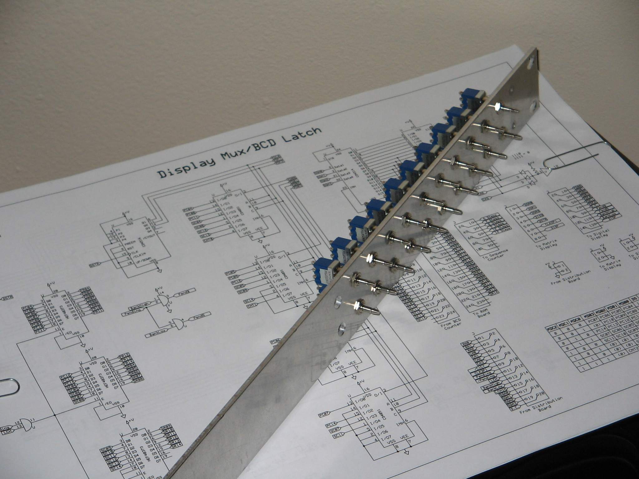 |
This switch panel should work out fine. I plan on soldering wires to each switch, connecting the wires to the debouncing circuitry on a separate small board, then interfacing that board to the flotilla of breadboards this process will require. The panel itself will be suspended horizontally towards the end of the breadboard fleet, and labeled with sharpie so I know which switch is which, which is a switch, let me tell you......
Keeping Track of Breadboards
Because prototyping this design is going to require several different breadboards, I've decided to keep track of which ICs are on which breadboard, and where on each breadboard those ICs are. This will help to easily find test points, etc.
 |  |
| Breadboard 1 | Breadboard 2 |
I've drawn up accurate representations of the breadboards using Visio. I've also constructed little IC representations that I can place in the positions the real ICs occupy on the breadboards.
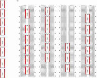
Breadboard 1 is the style of breadboard that I usually purchase from Jameco. The representation in the picture is how I have the System Clock/Control Counter breadboard configured.
 |
Actually, the picture of the actual Breadboard 1 diagram predates the diagram, but you can see, if you enlarge the picture, the diagram follows the placement of the ICs that are there.
 |
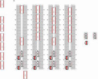
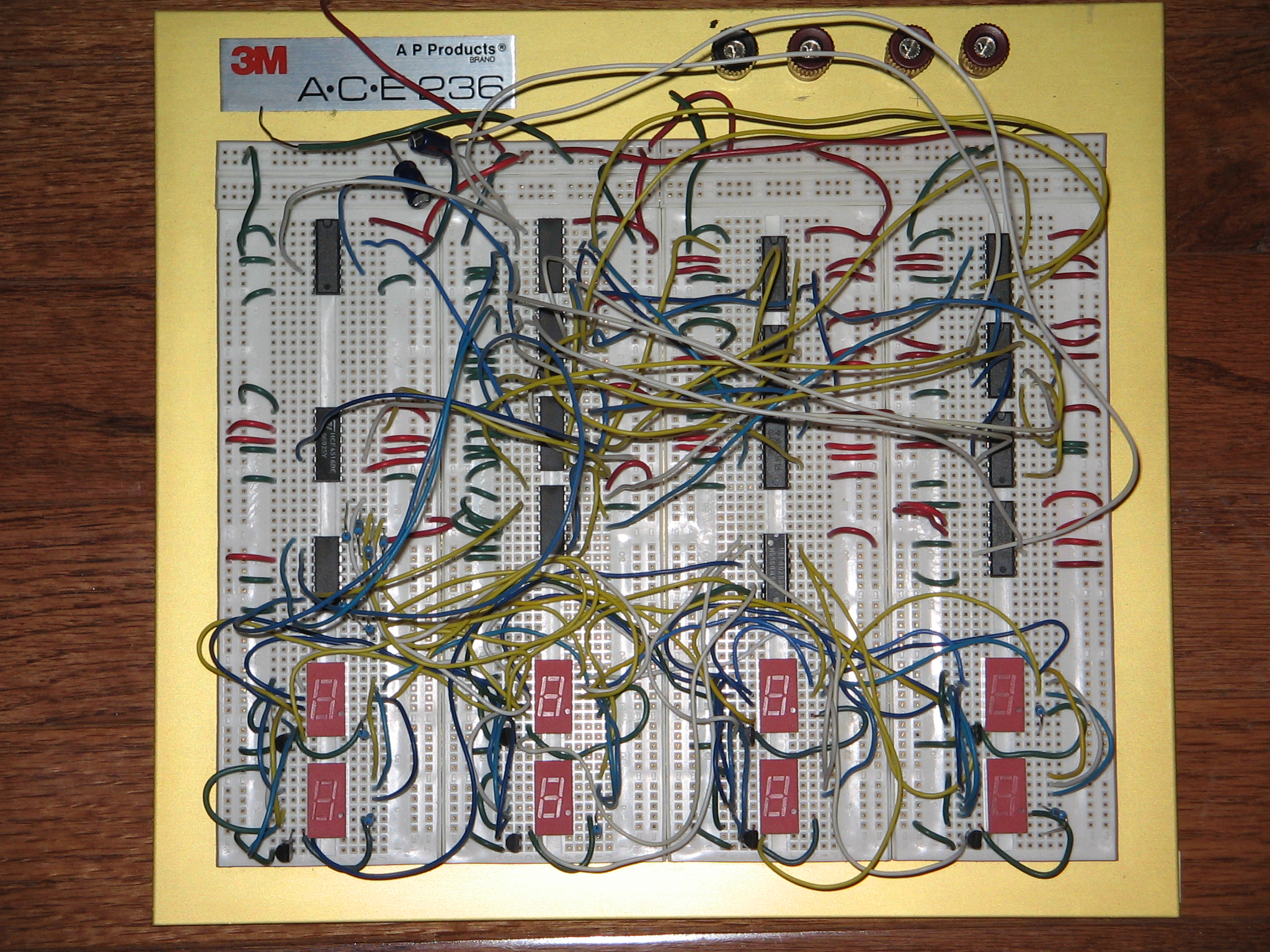
Breadboard 2 is a style of breadboard a friend from electro-music graciously donated to me. Nice breadboards - I don't know if those are even made anymore. In any event, it's a diagram of what I have done (at this writing) on the Digital Display Board, RAM BCD and Repeat BCD, which, as you can see, isn't a lot yet.
 |
The bottom portion of the board, with the wires and LED displays contains the circuitry that will wind up on the Digital Display board. Above that, the RAM BCD counters and the Repeat BCD counters are situated, along with the multiplexers required to drive the display. Those ICs are not yet wired up and the board is, at this writing, untested.
 |
Digital Display 04 December 2010
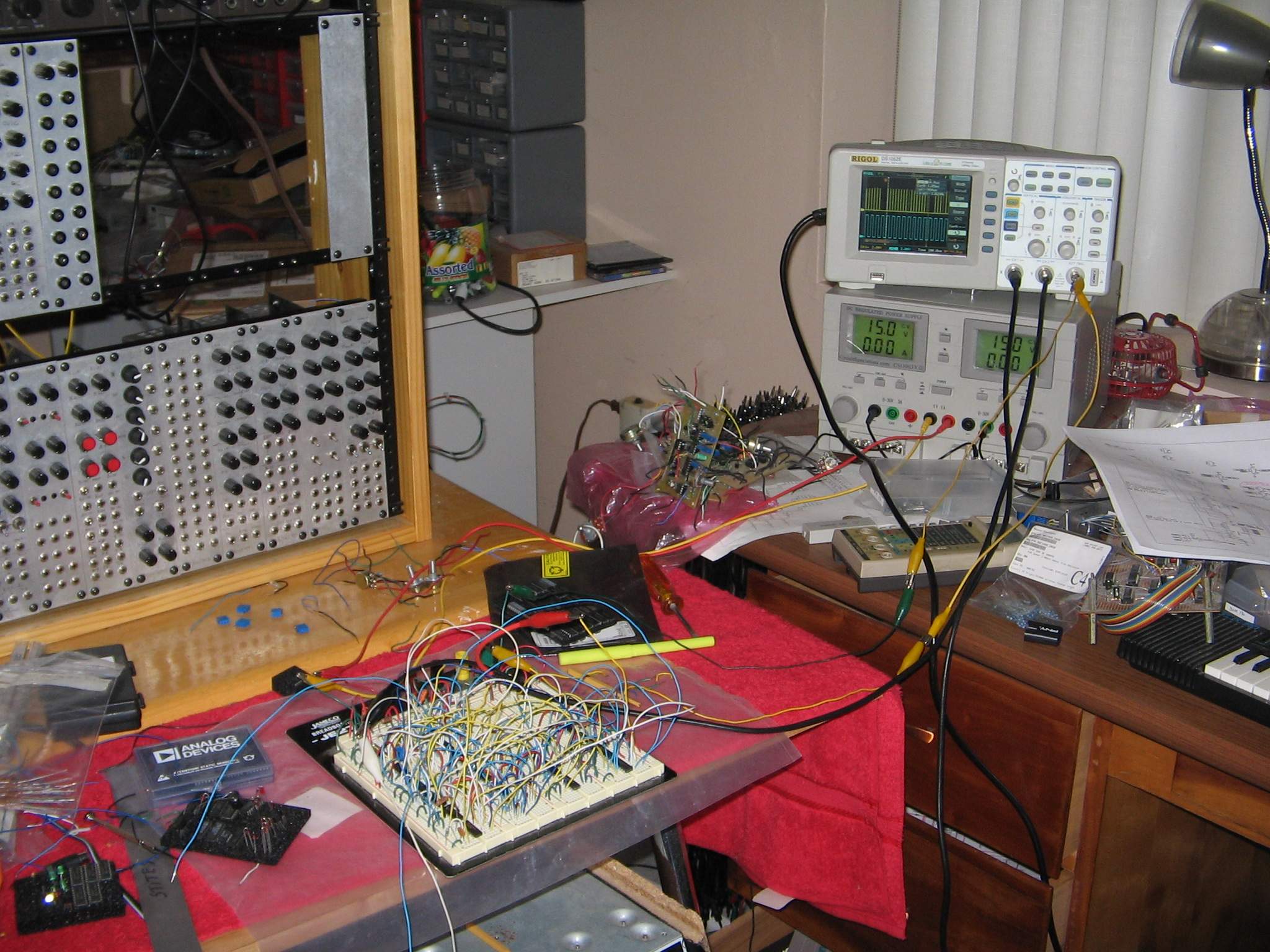
Today I finally got to the point of actually testing out the Digital Display Board/Mux circuitry. This circuit takes the output from all eight BCD counters, mutliplexes the BCD data, and sends the data to the Digital Display board.
 | 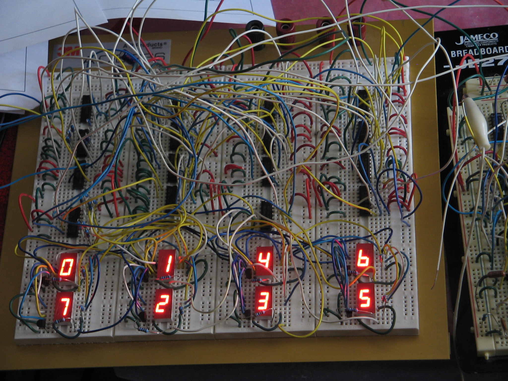 |
| Display and Control Counter Breadboards | Display Breadboard |
The picture on the left shows the Display breadboard and the Control Counter breadboard together. The display multiplexer uses the ANDed product of the CLK3P1 and C1CY signals from the Control Counter to clock the counter driving the multiplexers and, in its inverted form, this signal blanks the display driver so that there is no "bleed" from display to display.
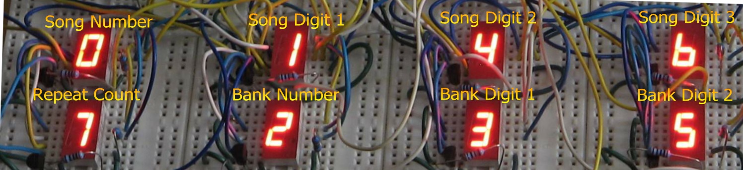 |
The design contains a total of eight digital LED displays: One is used for the Repeat Counter display, one is used to display the current Song Number, three are used to display the current Song Pattern, one is used to display the current Bank Number, and two more are used to display the current Bank Pattern.
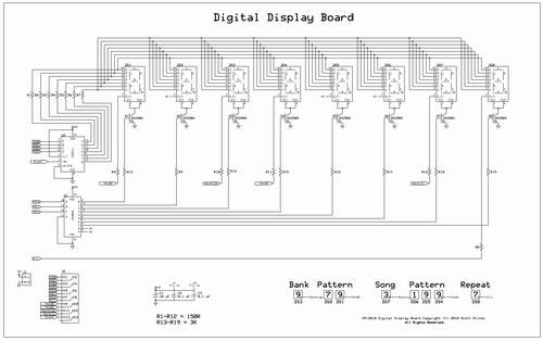 |
You can open or download the SM-2010 Digital Display Board schematic in PDF format by clicking the picture above. This is just the display board itself - I will provide schematics to the mux circuitry later.
One can see that this allows the digital displays to be built on a PCB, using a simple ribbon cable and power cable. Only a handful of parts are required to drive the displays from the signals provided on the ribbon cable.
MD00 through MD03 represent the multiplexed data from the eight BCD counters. They are used to provide data to the CD4511 display driver, which drives the eight seven-segment common cathode digital LED displays.
MDC0 through MDC2 are signals provided by the same mux counter that is driving four CD4051 multiplexers; these signals address the CD4028 which sequentially selects each display to receive the current data addressed by the mux counter. "Blank" is actually the inverted copy of the clock signal that drives the mux counter; when the counter goes high to advance the mux and display, the inverted copy drops low, turning the display driver off. This keeps propagation delay from allowing any signal to bleed from the current display to the next display while the count is advancing.
D.C., PendB, PendS, BankHigh and BankLow are sourced from other portions of the SM-2010 circuitry. These signals take advantage of the decimal point of each display to provide additional state-specific information such as if the current pattern displayed on the LED matrix is a song or a bank pattern, if the current pattern has its DC bit on, or if the pattern number has been manually advanced during pattern play and the current pattern will increment after it is finished playing all of its notes.
The displays are each updated once per millisecond, or at a rate of 1 kHz, and are on for 0.125 milliseconds each time they are addressed. This works out to a 1:8 duty cycle.
To be continued........