
The SM-2010 Control Counter
The Heart of the SM-2010
The Control Counter is the very heart, neural cortex, and endocrine system of the SM-2010. It exists to interface the pattern data to and from the RAM and to run the sequencer juice through the very arteries of the device.
This section contains no less than four CD4516 binary counters. Three of these counters are interlocked together to address the four least significant bits of RAM, provide row addressing for the matrix, and provide column addressing for the matrix.
The fourth counter is used to drive a CD4028 BCD to decimal decoder. This fourth counter is the true "control counter" from which the circuit derives its name; the output of the BCD decimal decoder steps through the sequence of events that synchronizes and controls the flow of data to and from RAM during a write or update cycle.
The Control Counter is driven from the various phases of the system clock and uses combinational logic to generate the read and write signals to the RAM and the shift register clock and control signals of the parallel to serial conversion. The Control Counter also synchronizes the data flow and provides the latch signal for the output latches.
The signals processed by the combinational logic are generated by the addressing counters, the various phases of the system clock, and a few external signals provided by other sections of the SM-2010.
The Control Counter and Pattern Data Flow
Figure 1 illustrates the Control Counter's role in the general scheme of pattern data flow and storage within the SM-2010.
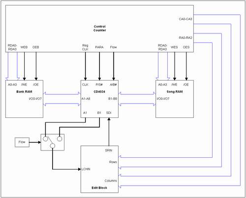 |
In Figure 1, the Control Counter can be seen interfacing with the RAM section of the SM-2010 as well as with the Edit Block portion of the SM-2010.
The RAM portion pictured consists of the Bank RAM and Song RAM ICs and the CD4034 8-Stage Static Bi-Directional Parallel/Serial Input/Output Bus Register (that's a mouth full!). Generally what the CD4034 does is accept parallel data from the RAM, convert it to serial data for circulation throughout the nether regions of the SM-2010, and transfer parallel data back to RAM.
The Edit Block is a section of circuitry within the SM-2010 that edits the serial data sent to it before sending it back to be stored into RAM. A SPDT solid state switch and the CD4034 work together to determine the direction of flow (either from Bank RAM to Song RAM or vice-versa).
It can be seen that the control counter is generating the following signals:
RDA0 through RDA3: This set of data addresses the four least significant RAM address bits.
WEB and WES: WEB is the Write Enable for Bank Ram; WES is Write Enable for Song RAM.
OEB and OES: OEB is Output Enable for Bank RAM; OES is Output Enable for Song Ram
CA0 through CA3: This set of data represents the column address data for the matrix.
R0 through R2: This set of data represents the row address data for the matrix.
Reg Clock: The Register Clock clocks the CD4034 in parallel or serial mode.
PARA: The parallel signal determines whether the CD4034 is in parallel or serial mode of operation.
Flow: The Flow signal determines which direction data is flowing, either from Bank to Song or Song to Bank. Notice that flow controls both the CD4034 and the solid state SPDT switch.
There are a few more details as to where all the signals go; for example, the Row and Column data is also used to determine what data needs to be latched by the output circuitry. But this is the majority of the jist I wish to impart in this discussion of the Control Counter.
The Control Counter is made up of a number of smaller blocks of functionality that perform each of these tasks. We have to start somewhere, so let us start with the three addressing counters.
Counters 1, 2 and 3
Counter 1, Counter 2 and Counter 3 provide the column (C0-C3), row (R0-R3), and least significant RAM address data (RDA0-RDA3). Combinations of signals generated by these three counters are also used in conjunction with other internal and external signals, to produce other timing signals generated by the Control Counter.
Generally though, it is enough right now to consider the addressing functions these three counters provide. In order to get a better understanding of these functions, refer to Figure 2.
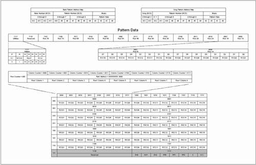 |
Figure 2 illustrates the RAM memory map of the SM-2010. At the top of the diagram the RAM addressing scheme is displayed.
There are two RAM sections: the Bank RAM and the Song RAM. Each of these RAM ICs has fourteen address bits and each supplies an eight bit wide data word.
The most significant ten bits are used to partition the RAM up into Banks, Songs and individual patterns. These most significant bits are addressed by the control interface which is supplied by other portions of the SM-2010 in BCD format.
The four least significant address bits are used to store pattern data, and these four bits are addressed by the Control Counter circuit (they are addressed by Counter 3 specifically but there’s a bit more to explain before we get into that). These four bits simultaneously address both RAM sections – when Bank RAM is at 1001, then Song RAM is also at 1001.
As mentioned before, the data word supplied by the RAM is eight bits wide. Each pattern is comprised of 128 bits. The four least significant address bits are addressed in binary from 0000 to 1111, which is a total of sixteen addresses. Therefore, a total of 128 data bits is addressed through this range (16 * 8 = 128).
The “Pattern Data” shown in Figure 2 bears this out. One can see that there are sixteen blocks of data in a single pattern. Because a row of notes contains sixteen notes, it takes two blocks of data to form a single row. One can see that the eight bits of data addressed by 0000 (D0 through D7) contains the bits for Row 1A (Row 1 Column 1 through Row 1 Column 8 or R1C1-R1C8). The eight bits of data addressed by 0001 contain the rest of the data for Row 1, which is labeled Row 1B. This data consists of Row 1 column 9 through Row 1 Column 16 (R1C9-R1C16).
This scheme continues on until address 1110 – the eight data bits of this word are not used (they’re marked “Reserved”). Address 1111 contains the eight bits of data required for the utility functions of the pattern: the length count (divisor) takes up the first three bits (D0-D2). The repeat data, which stores the number of repeats programmed into the pattern, takes up the next three bits (D3-D5). The next bit, D6, is not used, and D7 stores the D.C. on/off state for the pattern.
At the bottom of Figure 2 is a table that illustrates how the matrix is constructed. Think of it as looking at the matrix display itself; on the left hand side is the row number, in binary, and for every note in a row, there is a column number in binary at the top of the table. Above each row are the four least significant RAM address bits that hold the notes in the row. Again, note that each row actually is made up of two RAM addresses, because the row is sixteen bits long, but each RAM address only holds eight bits, so it requires two addresses to hold all of the data of a single row. The bottom row is marked in gray because it contains the contents of the unused memory address (1110) and the Utilities address (1111) and does not "appear" on the matrix display (the utilities functions are displayed elsewhere on the user interface in the form of various indicators).
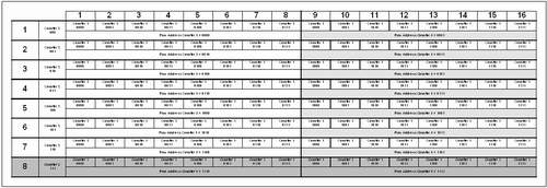 |
These binary column, row and address bits are generated by counters 1, 2 and 3. Figure 3 illustrates this more specifically. Note that the sixteen column numbers across the top of Figure 3 are addressed by Counter 1 from 0000 through 1111. The row numbers 1 through 8 are addressed by Counter 2 from 000 through 111. The RAM addresses are addressed by Counter 3 from 0000 through 1111.
Note the relationship between the counters: Counter 2 increments once for every sixteen counts of Counter 1. Counter 3 increments once for every eight counts of Counter 1.
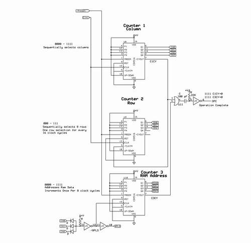 |
Each of the three counters is a CD4516 Presettable Up/Down counter. All three counters are configured to count up.
Counters 1 and 2 are arranged in synchronous cascade and are clocked by the CLK1 signal from the System Clock.
The Q1, Q2, Q3 and Q4 outputs of Counter 1 are labeled CA0, CA1, CA2 and CA3, respectively. These outputs are the Column Address control signals.
The Q1, Q2 and Q3 outputs of Counter 2 are labeled RA0, RA1 and RA2, respectively. These outputs are the Row Address control signals.
CA0, CA1 and CA2 are NANDed together by the Mickey Mouse Logic NAND gate U5; when all three of these signals are high, this represents the eighth count of Counter 1, and the output of U5 drops low. This low signal is labeled "/8 PLS", meaning "inverted eight pulse". When Counter 1 advances forward one more count, /8PLS goes high, clocking Counter 3. Thus, Counter 3 is clocked every eighth count of Counter 1. Incidentally, /8PLS is also inverted by U5 to form the 8PLS signal, which is used elsewhere (to be discussed shortly).
The Q1, Q2, Q3 and Q4 outputs of Counter 3 are labeled RDA0, RDA1, RDA2 and RDA3, respectively. These outputs are used to address the lowest significant bits of both the Bank and Song RAM ICs.
When a CD4516 reaches the terminal count of 1111, the /CYOUT signal present at pin 7 of the IC drops low. This is the carry-out signal. Starting at a count of 0000, it takes 128 counts for both Counter 1 and Counter 3 to reach 1111 (remember, Counter 3 clocks at every eighth count of Counter 1, so 16*8=128). The carry-out signal of Counter 1 is labeled C1CY and the carry-out signal of Counter 3 is labeled C3CY. When both of these CY bits drop low, pin 4 of OR gate U11 drops low, which produces a short, positive going pulse output from pin 6 of U5 because this section of U5 is configured as a Schmitt trigger one-shot. This short pulse signifies that the operation is complete (OPC) - the count has reached 128. The OPC pulse signal is used elsewhere in the Control Counter to indicate that the full count has occurred. It's imperative to be able to detect when a 128 pulse count from 0000 on all counters to 1111 on both Counter 1 and Counter 3 has occurred - this is used to synchronize a write to RAM or write to latch function. The OPC pulse is used to determine when the operation has completed. The operation is synchronized through the use of the Preset signal.
All three of the counters are preset to a count of 1111 when the Preset signal goes high. This allows the counters to all start their 128 count at the first clock which rolls the counters over to 0000. The Preset signal originates from another section of the Control Counter, which will be discussed shortly.
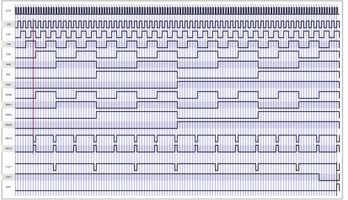 |
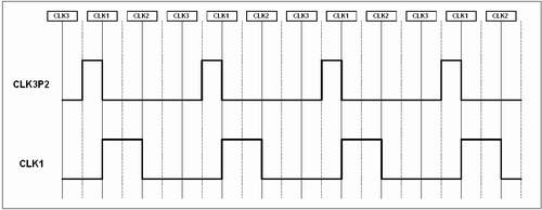
Figure 5 is a timing diagram depicting the outputs of the counters and the other signals from Figure 4. The timing diagram spans exactly 128 pulses after the Preset signal has set the counters all to a count of 1111 and the first pulse of CLK1 has rolled the counters over to 0000. The vertical blue lines indicate each pulse of the CLK1 signal.
What becomes immediately apparent is that there is some duplication of signals:
- CA3 = RDA0
- RA0 = RDA1
- RA1 = RDA2
- RA2 = RDA3
In other words, all of the RAM address bits are already generated by Counter 1 and Counter 2; the function could be accomplished by using only two counters.
Why then did I choose to go with three counters? There are two reasons. First, in order to generate the OPC pulse, I would have had to combine CA3, RA0, RA1, and RA2 together. This would not have been all that difficult, but, the room taken by the four diodes and one resistor would have bitten into economy of space.
The second reason was, mainly, it is much easier to keep track of the signals if they are broken out into discrete duplicates of each other, and the outputs are fanned to enough places to make it not too bad of an idea to keep the signals separate for improved drive capability. I may eventually end up using two counters, but I rather prefer using the three counters at this point.
There are probably a number of ways this whole thing could be done - downcount could be used instead of up count and things could be rearranged to accomodate that. But I went through so many iterations of the Control Counter, I feel I need to put a fork in it and call it done if it is working. It gets more complicated downstream and there are other fish to fry......
The Control Sequencer
Counters 1, 2 and 3 run all the time; they never stop except when, perhaps, they’re told to line up behind the yellow line, and then, only briefly will they do that. This is essential to keep the lights on, so to speak, for the matrix display. The matrix displays the data as it is pulled from RAM, converted to serial format, and paraded through its LEDs so it can give us humans some idea of what is happening with the device. Of course, the counters provide the matrix display with row and column information so that it knows what data is currently in its grip, and which LEDs it should light up at any given time. But, this isn’t about the matrix display, this about the control sequencer.
The point is, the counters are always running. They can be at any count at any time. As was discussed previously, the RAM addressing is pretty damn rigid – in a store event, the right bits have to go to exactly the right location in RAM in order for a pattern to be usefully saved. The same applies to the output latches; the output latch must store the right information at exactly the right time in order for the output gates and triggers to have any semblance of coherence at all. So, when the time comes to write something to RAM or to the output latch, the counters need to be corralled, placed in a known state, then get the bejesus clocked out of them for the exact number of counts while all the time telling the RAM to write the data at exactly the right time as the data goes stampeding by. Getting all the ducks lined up in a row is the function of the Preset signal discussed in the Counters section earlier in this page.
But, something has to tell that Preset to fire. Not only that, something has to be able to tell when exactly 128 clock pulses have occurred, when to send a write pulse to the RAM, when to tell the RAM to push out its contents onto the data bus, when to clock the shift register, when to latch the latches, and when to shut the iron off before going on vacation. All of these events have to occur at the right time and only when we want them to occur.
So, yes, at various points we want all of this stuff to happen. When we want it to happen will be discussed later; how we want this to happen will be discussed right here and now.
What we are looking at is a sequence of events that we want to occur. Hmmm….sequence…sequencer! Ha! That’s what we need – a sequencer that sequences a bunch of stuff to happen in sequence. And that is what the Control Sequencer is for. We want to trigger it to do something, have it do that thing, and then have it wait for the next time we want to trigger it and have it do the same thing again.
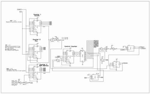 |
This gets really involved at this point; if you want to follow along, it will help to either print out Figure 6 or open it up in another window or on a second monitor, if you've got one. Figure 6 is a schematic of the basic guts of the Control Sequencer. I’ve included Counters 1, 2 and 3 with the schematic to detail the interaction the control sequencer has with the counters.
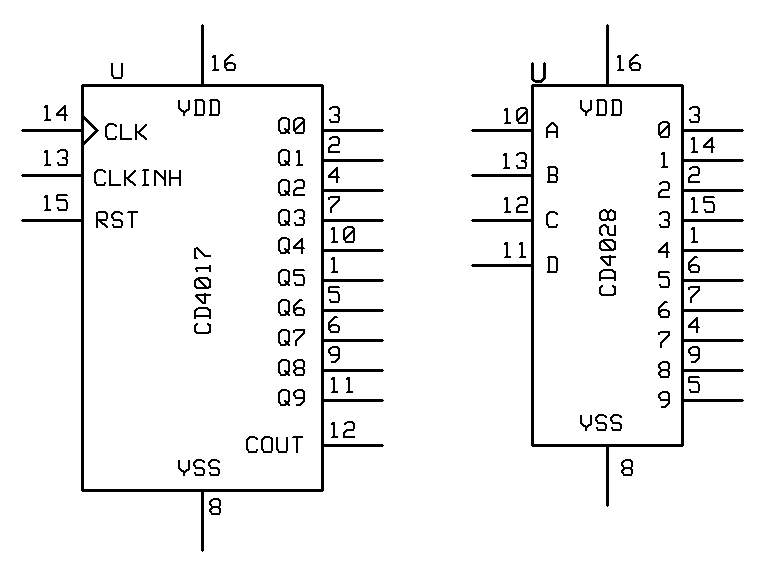
You will see there is an additional counter added, a CD4516 labeled as the “Control Counter”, which is what it does. Its outputs address the CD4028 BCD to Decimal Decoder and count through all of the control steps.
Tried the Baby 10 Sequencer? Use a CD4028 to build a "Toddler 10"!
Check out the CD4028: it has the same number of outputs that a CD4017 has, plus it is addressable. This means you can drive it with a counter with far more capabilites than a CD4017 and make that bad boy jump through hoops. With this simple change you can add sequence up, sequence down, and jam inputs while still keeping things simple.
Drive it with a CD4510 BCD Up/Down counter to keep it a single ten step sequencer, or use two (or more) and drive it with a CD4516. Hint: the 'D' line can act as a chip enable. Check out the ARP1 601 sequencer sometime for ideas....
The CD4028 is a wonderful little device. If you’re not familiar with it, it could be somewhat compared to a CD4017: it has ten outputs, and, when addressed with BCD code, only one output will be high at any given time. Unlike a CD4017, it is not clocked, but rather is addressed: whatever address is sent to its inputs will send the addressed bit high. I, for the life of me, can’t understand why people flock to the CD4017 to build a sequencer when they could add a counter driving this device and make a very simple sequencer that could really jump through some hoops (ARP used it in their 1601 Sequencer, for crying out loud). But, I digress…..
The Control Counter is used to clock the CD4028 outputs through a specific set of states. Note that the last state is called “Hold”, and that is the one we’ll look at first, because it is how the Control Sequencer is able to wait around until told what to do.
Let’s say the CD4516 starts its count at 0000; while it is at 0000, the ‘0’ output at pin 3 of the 4028 is high, and the rest of its outputs are low. Then the CD4516 counts to 0001 and the “1” output at pin 14 of the 4028 goes high while the “0” output of the CD4028 goes low (the high output shifts just like a step sequencer). This happens with each successive output of the CD4028 as the CD4516 counts up until the CD4516 reaches count 0111, which shifts the high signal to the “7” output at pin 4. This is the “Hold” step.
Notice that the Hold step is connected to the input of an OR gate, U11. For now, don’t worry about the other input to the OR gate – this Hold level is enough to force the output of the OR gate (U11, pin 10) high. The output of the OR gate is connected to the “/CLKIN” input of the Control Counter U12 Pin 5. When “/CLKIN” is high on a CD4516, it ignores any further clock pulses. In other words, the Control Counter cannot advance to the next count, so the CD4028 output cannot shift any more and things have now come to a stop. The Control Sequencer will not advance any further and will hold in that state until something wakes it up and tells it to move on. Something will have to bring Hold low before that can happen.
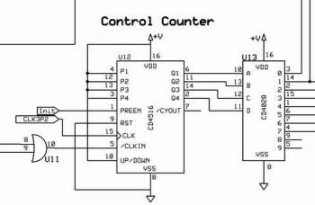
That “something” comes in the form of the INIT pulse. The INIT pulse is used to initialize the Control Sequencer and allow it to do its thing. The INIT pulse is a very high profile signal in the scheme of things. It comes from some other function of the SM-2010 when that function requires either a write to RAM or a write to the output latch. The INIT pulse is connected directly to the Control Counter’s preload pin. When, for whatever reason, an INIT pulse is generated, the INIT pulse preloads (forces) the outputs of the Control Counter to 1111. Of course, these outputs address the CD4028, and when the CD4028 sees the input code “1111”, the 9 count goes high on pin 5. You will notice pin 5 is connected to nothing. What’s important in this case is that all of the connected outputs of the CD4028 are now low. This includes the Hold output. Because the hold output is low, the Control Counter will now begin counting from 1111 to 0000 and on up again with each rising edge of its input clock as soon as the INIT pulse drops low again (which is pretty damn quick). This allows the Control Sequencer to step through all of its states again until it gets to the Hold state, whereupon it will hold again, waiting for the next INIT pulse, whenever that should come.
At this point, I will draw attention to just exactly what is clocking the Control Counter. Note that the signal connected to the CD4516 is labeled “CLK3P2”. This is the second phase of the third phase of the system clock. What this means is that this signal is ensured to rise and full immediately before CLK1 rises. Remember, CLK1 is driving Counters 1, 2 and 3. The effect of this is that the Control Sequencer changing state is the last thing to occur right before the address, row and column counters change state. In other words, the Control Sequencer sets up the conditions, then allows the address counters to fulfill those conditions. Remember that. It’s important.
To further unwrap the layers of what’s going on here, let’s consider what the Control Sequencer is ultimately supposed to do: it is either requested to write a pattern to RAM or to write a column of data to the output latch. To be more specific, if it performs a write function, that will always be followed by a read function, and the read function will always write to RAM, but more of as a sort of write-to-temporary memory moment. That will all be explained later; right now, I just need to show what happens when the Control Sequencer is requested to write to RAM.
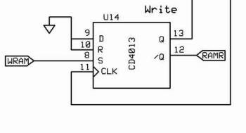
When the Control Sequencer is requested to write a pattern to RAM, a second signal accompanies the INIT pulse: the WRAM pulse (or “Write to RAM pulse”). Note that the WRAM pulse is connected to the pin 8 Set input of flip flop U14. This short, high pulse causes the Q output at Pin 13 of U14 (labeled "Write" in Figure 6) to go high.
Meanwhile, the INIT pulse has occurred simultaneously and the Control Sequencer has sprung to action. It counts through the state “WriteInit” (Write Initialize, which is explained later) to the “Write” state. Notice that “Write”, which is now high, is ANDed with the high Q output of U14 by the AND gate U16. Because “Write” his high, and U14 pin 3 is high, the output of the AND gate, U14, pin 3, is also brought high. This high output is ORed with another signal to be discussed shortly by U11. The transition from low to high on pin 11, the output of the OR gate is inverted and fed to a Schmitt trigger one shot formed from U15 to produce a very short pulse on the output of the one shot, U15 pin 4.
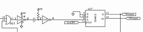
This short, positive going pulse sets the pin 13 Q output of flip flop U17 high. This Q signal on pin 13 of U17 is the Preset signal which is connected to Counters 1, 2, and 3. When Preset goes high, Counters 1, 2 and 3 are all forced to output “1111” and they can no longer be clocked while Preset is high. Remember, Preset was told to go high by the Control Sequencer, which only does things on the second half of the third phase of the system clock.
So, Preset goes high, the counters jump to “1111” and, after that, the CLK1 signal hits the counters – they can’t move because Preset is still high. Note that the clock input of flip flop U14 (pin 11) is connected to CLK3P1, or the first half of the third phase of the system clock. When this signal comes around, after our aborted CLK1 signal, Preset drops low and the next CLK1 signal will clock the counters over from 1111 to 0000, and the game is on.
Ah, but look at what has happened in the meantime, because not only is Preset connected to the counters, but it is also connected to the Set input of U14, pin 6. This causes the Q output, pin 1, of U14 to go high. Notice that the signal output of this Q pin is labeled “Hold128”. And that is exactly what it does – it causes things to hold for exactly 128 counts of the system clock. Hold128 is connected, through the U11 OR gate to the CLKIN input of the CD4516 (this is the signal I mentioned would be explained later). So, now the Sequence Counter again is prevented from reacting to any clock signals; it is now holding the Write output high.
So, what has happened is the Write output has gone high, which presets the counters and causes the sequencer to hold in the Write state. In the meantime, the counters have been preset to 1111 and hold until preset goes low. Then preset is allowed to go low, and the next CLK1 pulse to come along will roll the counters over to 0000.
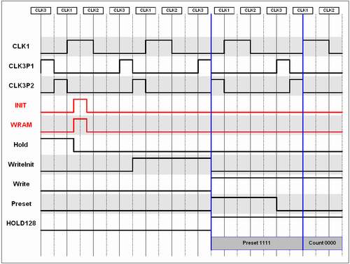 |
The counters will count up exactly 128 steps (until Counter 1 and Counter 3 each are at 1111 at the same time). When that state occurs, the OPC pulse is generated. OPC is connected to the clock input (pin 3) of U14, which causes Hold128 to clock low. When Hold128 clocks low, the next CLK3P3 signal to come along will step the Control Sequencer to the next state, and the write to RAM cycle is completed.
To be continued.......